

IEEE AC and DC Exciters
The rotating-exciter models of IEEE Std 421.5 available in RAMSES: three alternator-supplied (AC) types and one DC type.
The EXC sub-record these models are entered with, and the table of IEEE model variants, are on the Exciter Models page.
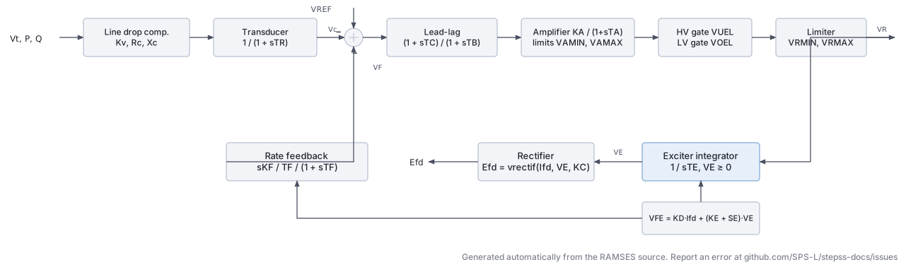
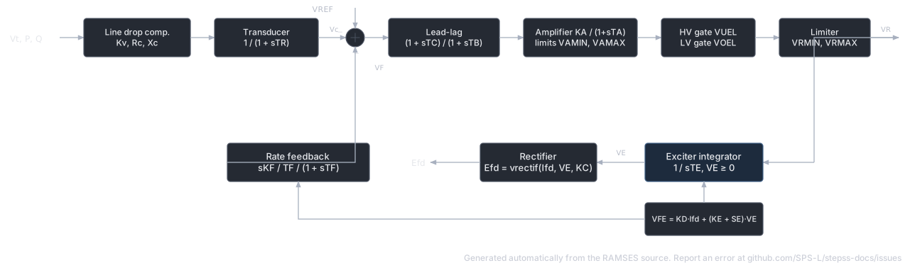
The AC1A is a rotating AC exciter with a self-excited field winding and non-linear saturation. It corresponds to IEEE Std 421.5-2016 Type AC1A. The generator terminal voltage is compensated for line drop and filtered before being compared with the reference. An AC alternator supplies the field through a rectifier whose output depends on the commutation voltage and field current .
Mathematical Description
Section titled “Mathematical Description”The voltage regulator processes the error signal through a lead-lag network and a limited amplifier:
The AC exciter integrator with saturation and demagnetization:
The derivative feedback (rate feedback) path:
where is the saturation function interpolated from the two-point saturation characteristic and .
Signal Flow
Section titled “Signal Flow”- Line drop compensation (
algeq): - Voltage measurement filter (
tf1p): with time constant - AVR summation (
algeq): - Lead-lag compensator (
tf1p1z): with - Amplifier with limits (
tf1plim): with gain , time constant , limits - UEL high-value gate (
max1v1c): - OEL low-value gate (
min1v1c): - Output limiter (
lim): - Exciter integrator (
inlim): - Saturation computation (
algeq): from , , - Rectifier output (
algeq): - Derivative feedback (
tfder1p): with gain , time constant
Parameters
Section titled “Parameters”| Parameter | Description | Unit/Type |
|---|---|---|
Kv | Voltage compensation gain | pu |
Rc | Resistance for line drop compensation | pu |
Xc | Reactance for line drop compensation | pu |
TR | Voltage transducer time constant | s |
KA | Voltage regulator gain | pu |
TA | Voltage regulator time constant | s |
TB | Lead-lag denominator time constant | s |
TC | Lead-lag numerator time constant | s |
VAMAX | Maximum regulator output | pu |
VAMIN | Minimum regulator output | pu |
KE | Exciter constant (self-excitation term) | pu |
TE | Exciter time constant | s |
KF | Rate feedback gain | pu |
TF | Rate feedback time constant | s |
VRMAX | Maximum field voltage | pu |
VRMIN | Minimum field voltage | pu |
VE1 | Saturation factor voltage point 1 | pu |
SE1 | Saturation factor at | pu |
VE2 | Saturation factor voltage point 2 | pu |
SE2 | Saturation factor at | pu |
KC | Commutation factor (rectifier regulation) | pu |
KD | Demagnetization factor | pu |
VUEL | UEL input signal | pu |
Variants
Section titled “Variants”| Model | Description |
|---|---|
AC1A | Base model, IEEE Type AC1A |
AC1A_MAXEX2 | Adds MAXEX2 field current limiter; VOEL moves to reference summation point (LV gate removed) |
AC1A_RETRO | Retrofit variant with internal PSS4B; uses first-order AVR without separate exciter block |
AC1A_RETRO_PSS4B | Retrofit variant with external PSS4B speed input |
Usage Example
Section titled “Usage Example”Show the data record
SYNC_MACH g1 g1 # FP FQ P Q: share of the power-flow injection (FP, FQ) or initial power (P in MW, Q in Mvar) 1. 1. 0. 0. # SNOM: Nominal apparent power, used as base power in the machine model (MVA) 800. # Pnom: Nominal active power of the turbine, used as base power for the turbine model (MW) 760. # H: Inertia constant (s) 3. # D: Damping coefficient (usually set to zero when the damper windings are modelled) (pu) 0. # IBRATIO: Field current base ratio I_fB^mac/I_fB^exc (see above) (pu) 0.95 # TYPE_MOD: Parameter format keyword: RL or XT (case-insensitive) XT # Xl: Leakage reactance L_l (pu) 0.15 # Xd: d-axis synchronous reactance (pu) 1.1 # X'd: d-axis transient reactance (must be smaller than Xd) (pu) 0.25 # X"d: d-axis subtransient reactance (pu) 0.2 # Xq: q-axis synchronous reactance (pu) 0.7 # X'q: q-axis transient reactance (pu) * # X"q: q-axis subtransient reactance (pu) 0.2 # m: Saturation coefficient (set to 0 to neglect saturation) 0.1 # n: Saturation exponent (ignored when m = 0) 6.0257 # Ra: Armature resistance (pu) 0. # T'do: d-axis open-circuit transient time constant (s) 5.00 # T"do: d-axis open-circuit subtransient time constant (s) 0.05 # T'qo: q-axis open-circuit transient time constant (s) * # T"qo: q-axis open-circuit subtransient time constant (s) 0.1EXC AC1A # Kv: weight of the terminal voltage in the measured voltage |Kv V + (Rc+jXc) I|; 1 = terminal voltage 1. # Rc: Resistance for line drop compensation 0. # Xc: Reactance for line drop compensation 0. # TR: Voltage transducer time constant 0.02 # KA: Voltage regulator gain 200.0 # TA: Voltage regulator time constant 0.02 # TB: Lead-lag denominator time constant 10.0 # TC: Lead-lag numerator time constant 1.0 # VAMAX: Maximum regulator output 7.32 # VAMIN: Minimum regulator output -7.32 # KE: Exciter constant (self-excitation term) 1.0 # TE: Exciter time constant 1.0 # KF: Rate feedback gain 0.03 # TF: Rate feedback time constant 1.0 # VRMAX: upper limit of the regulator output after the UEL and OEL gates (pu) 6.03 # VRMIN: lower limit of the regulator output after the UEL and OEL gates (pu) -5.43 # VE1: Saturation factor voltage point 1 4.18 # SE1: Saturation factor at V_E1 0.1 # VE2: Saturation factor voltage point 2 3.14 # SE2: Saturation factor at V_E2 0.033 # KC: Commutation factor (rectifier regulation) 0.2 # KD: Demagnetization factor 0.38 # VUEL: UEL signal into the high-value gate; a large negative value disables it (pu) -99999TOR CONSTANT;The AC4A is a simplified static representation of an AC exciter system with an inner-loop voltage-dependent output limit. It corresponds to IEEE Std 421.5-2016 Type AC4A. The upper output limit is a function of field current: .


Mathematical Description
Section titled “Mathematical Description”
The variable upper limit is updated algebraically at each time step, making AC4A a time-varying limited integrator system.
Signal Flow
Section titled “Signal Flow”- Line drop compensation (
algeq): from terminal measurements - Voltage measurement filter (
tf1p): with - AVR summation (
algeq): - Input limiter (
lim): - Lead-lag (
tf1p1z): with - UEL high-value gate (
max1v1c): - Variable upper limit (
algeq): - Variable-limit amplifier (
tf1pvlim): with , , limits
Parameters
Section titled “Parameters”| Parameter | Description | Unit/Type |
|---|---|---|
Kv | Voltage compensation gain | pu |
Rc | Line drop compensation resistance | pu |
Xc | Line drop compensation reactance | pu |
TR | Measurement filter time constant | s |
VIMAX | Maximum input error signal | pu |
VIMIN | Minimum input error signal | pu |
TC | Lead numerator time constant | s |
TB | Lag denominator time constant | s |
VUEL | UEL signal value | pu |
KA | Regulator gain | pu |
TA | Regulator time constant | s |
VRMAX | Maximum output (at zero field current) | pu |
VRMIN | Minimum output | pu |
KC | Field current derating factor | pu |
Variants
Section titled “Variants”| Model | Description |
|---|---|
AC4A | Base model, IEEE Type AC4A, no PSS or OEL |
Usage Example
Section titled “Usage Example”Show the data record
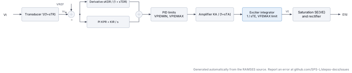
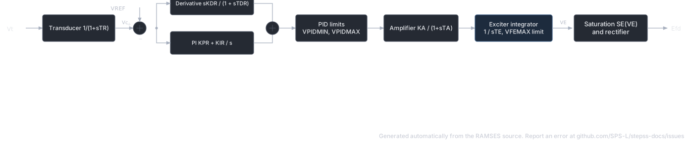
SYNC_MACH g1 g1 # FP FQ P Q: share of the power-flow injection (FP, FQ) or initial power (P in MW, Q in Mvar) 1. 1. 0. 0. # SNOM: Nominal apparent power, used as base power in the machine model (MVA) 800. # Pnom: Nominal active power of the turbine, used as base power for the turbine model (MW) 760. # H: Inertia constant (s) 3. # D: Damping coefficient (usually set to zero when the damper windings are modelled) (pu) 0. # IBRATIO: Field current base ratio I_fB^mac/I_fB^exc (see above) (pu) 0.95 # TYPE_MOD: Parameter format keyword: RL or XT (case-insensitive) XT # Xl: Leakage reactance L_l (pu) 0.15 # Xd: d-axis synchronous reactance (pu) 1.1 # X'd: d-axis transient reactance (must be smaller than Xd) (pu) 0.25 # X"d: d-axis subtransient reactance (pu) 0.2 # Xq: q-axis synchronous reactance (pu) 0.7 # X'q: q-axis transient reactance (pu) * # X"q: q-axis subtransient reactance (pu) 0.2 # m: Saturation coefficient (set to 0 to neglect saturation) 0.1 # n: Saturation exponent (ignored when m = 0) 6.0257 # Ra: Armature resistance (pu) 0. # T'do: d-axis open-circuit transient time constant (s) 5.00 # T"do: d-axis open-circuit subtransient time constant (s) 0.05 # T'qo: q-axis open-circuit transient time constant (s) * # T"qo: q-axis open-circuit subtransient time constant (s) 0.1EXC AC4A # Kv: weight of the terminal voltage in the measured voltage |Kv V + (Rc+jXc) I|; 1 = terminal voltage 1. # Rc: Line drop compensation resistance 0. # Xc: Line drop compensation reactance 0. # TR: Measurement filter time constant 0.02 # VIMAX: Maximum input error signal 8.0 # VIMIN: Minimum input error signal -8.0 # TC: Lead numerator time constant 1.0 # TB: Lag denominator time constant 10.0 # VUEL: UEL signal into the high-value gate; a large negative value disables it (pu) -99999 # KA: Regulator gain 200.0 # TA: Regulator time constant 0.015 # VRMAX: Maximum output (at zero field current) 4.44 # VRMIN: Minimum output -4.44 # KC: Field current derating factor 0.0TOR CONSTANT;The AC8B is a rotating AC exciter with a PID voltage regulator (rather than the proportional-integral amplifier of earlier types). It corresponds to IEEE Std 421.5-2016 Type AC8B. The PID structure, proportional gain , integral gain , and derivative gain , provides improved transient response compared to Type AC1A.
Mathematical Description
Section titled “Mathematical Description”The PID voltage regulator:
The AC exciter with variable limits based on maximum field excitation voltage :
Signal Flow
Section titled “Signal Flow”- Voltage measurement (
tf1p): with - Error signal (
algeq): - PID derivative part (
tfder1p): with gain - PID proportional-integral (
pictl): with , - PID sum (
algeq): , limited to - Amplifier (
tf1plim): with , - Exciter integrator (
invlim): with variable limits from - Saturation and rectification (
algeq): ,
Parameters
Section titled “Parameters”| Parameter | Description | Unit/Type |
|---|---|---|
Kv | Voltage compensation gain | pu |
Rc | Line drop resistance | pu |
Xc | Line drop reactance | pu |
TR | Measurement time constant | s |
KPR | PID proportional gain | pu |
KIR | PID integral gain | pu/s |
KDR | PID derivative gain | pu·s |
TDR | PID derivative filter time constant | s |
VPIDMAX | PID output upper limit | pu |
VPIDMIN | PID output lower limit | pu |
KA | Amplifier gain | pu |
TA | Amplifier time constant | s |
VRMAX | Maximum regulator output | pu |
VRMIN | Minimum regulator output | pu |
KC | Rectifier commutation factor | pu |
KD | Demagnetization factor | pu |
KE | Exciter self-excitation constant | pu |
TE | Exciter time constant | s |
VFEMAX | Maximum field excitation voltage | pu |
VEMIN | Minimum exciter output | pu |
VE1 | Saturation voltage point 1 | pu |
SE1 | Saturation factor at | pu |
VE2 | Saturation voltage point 2 | pu |
SE2 | Saturation factor at | pu |
Variants
Section titled “Variants”| Model | Description |
|---|---|
AC8B | Base model, IEEE Type AC8B |
AC8B_PSS3B_lim | Adds PSS3B dual-input stabilizer and integral OEL + SCL (stator current limiter) |
AC8B_lim | Adds integral OEL and SCL without PSS |
Usage Example
Section titled “Usage Example”Show the data record
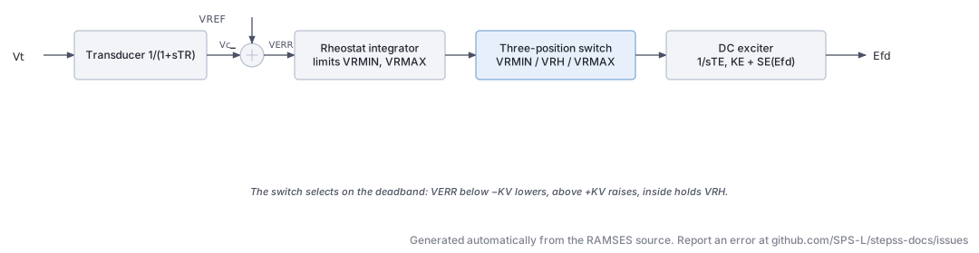
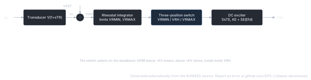
SYNC_MACH g1 g1 # FP FQ P Q: share of the power-flow injection (FP, FQ) or initial power (P in MW, Q in Mvar) 1. 1. 0. 0. # SNOM: Nominal apparent power, used as base power in the machine model (MVA) 800. # Pnom: Nominal active power of the turbine, used as base power for the turbine model (MW) 760. # H: Inertia constant (s) 3. # D: Damping coefficient (usually set to zero when the damper windings are modelled) (pu) 0. # IBRATIO: Field current base ratio I_fB^mac/I_fB^exc (see above) (pu) 0.95 # TYPE_MOD: Parameter format keyword: RL or XT (case-insensitive) XT # Xl: Leakage reactance L_l (pu) 0.15 # Xd: d-axis synchronous reactance (pu) 1.1 # X'd: d-axis transient reactance (must be smaller than Xd) (pu) 0.25 # X"d: d-axis subtransient reactance (pu) 0.2 # Xq: q-axis synchronous reactance (pu) 0.7 # X'q: q-axis transient reactance (pu) * # X"q: q-axis subtransient reactance (pu) 0.2 # m: Saturation coefficient (set to 0 to neglect saturation) 0.1 # n: Saturation exponent (ignored when m = 0) 6.0257 # Ra: Armature resistance (pu) 0. # T'do: d-axis open-circuit transient time constant (s) 5.00 # T"do: d-axis open-circuit subtransient time constant (s) 0.05 # T'qo: q-axis open-circuit transient time constant (s) * # T"qo: q-axis open-circuit subtransient time constant (s) 0.1EXC AC8B # Kv: weight of the terminal voltage in the measured voltage |Kv V + (Rc+jXc) I|; 1 = terminal voltage 1. # Rc: Line drop resistance 0. # Xc: Line drop reactance 0. # TR: Measurement time constant 0.02 # KPR: PID proportional gain 1.0 # KIR: PID integral gain 5.0 # KDR: PID derivative gain 0.1 # TDR: PID derivative filter time constant 0.1 # VPIDMAX: RAMSES 3.84 applies this value as the LOWER limit of the PID output (pu) -8.0 # VPIDMIN: RAMSES 3.84 applies this value as the UPPER limit of the PID output (pu) 8.0 # KA: Amplifier gain 1.0 # TA: Amplifier time constant 0.1 # VRMAX: Maximum regulator output 6.5 # VRMIN: Minimum regulator output -6.5 # KC: Rectifier commutation factor 0.2 # KD: Demagnetization factor 1.0 # KE: Exciter self-excitation constant 1.0 # TE: Exciter time constant 0.5 # VFEMAX: Maximum field excitation voltage 6.5 # VEMIN: Minimum exciter output 0.0 # VE1: Saturation voltage point 1 4.0 # SE1: Saturation factor at V_E1 0.3 # VE2: Saturation voltage point 2 3.0 # SE2: Saturation factor at V_E2 0.1TOR CONSTANT;The DC3A represents a non-continuously acting (rheostat-type) DC excitation system. It corresponds to IEEE Std 421.5-2016 Type DC3A. Rather than a proportional amplifier, it uses a three-position switch (VRMIN / VRH / VRMAX) driven by an integrator that holds the rheostat position . The switch position is determined by whether the error signal falls inside or outside a deadband .
Mathematical Description
Section titled “Mathematical Description”
The rheostat integrator:
The three-position switch:
The DC exciter with saturation:
Parameters
Section titled “Parameters”| Parameter | Description | Unit/Type |
|---|---|---|
Kvcomp | Voltage compensation gain | pu |
Rc | Line drop resistance | pu |
Xc | Line drop reactance | pu |
TR | Measurement time constant | s |
TRH | Rheostat traversal time | s |
KV | Sensitivity of non-continuously acting controller | pu |
VRMAX | Maximum field voltage | pu |
VRMIN | Minimum field voltage | pu |
TE | Exciter time constant | s |
KE | Exciter self-excitation constant | pu |
E1 | Saturation voltage point 1 | pu |
SE1 | Saturation factor at | pu |
E2 | Saturation voltage point 2 | pu |
SE2 | Saturation factor at | pu |
Variants
Section titled “Variants”| Model | Description |
|---|---|
DC3A | Base model, IEEE Type DC3A, non-continuously acting rheostat controller |
Usage Example
Section titled “Usage Example”Show the data record
SYNC_MACH g1 g1 # FP FQ P Q: share of the power-flow injection (FP, FQ) or initial power (P in MW, Q in Mvar) 1. 1. 0. 0. # SNOM: Nominal apparent power, used as base power in the machine model (MVA) 800. # Pnom: Nominal active power of the turbine, used as base power for the turbine model (MW) 760. # H: Inertia constant (s) 3. # D: Damping coefficient (usually set to zero when the damper windings are modelled) (pu) 0. # IBRATIO: Field current base ratio I_fB^mac/I_fB^exc (see above) (pu) 0.95 # TYPE_MOD: Parameter format keyword: RL or XT (case-insensitive) XT # Xl: Leakage reactance L_l (pu) 0.15 # Xd: d-axis synchronous reactance (pu) 1.1 # X'd: d-axis transient reactance (must be smaller than Xd) (pu) 0.25 # X"d: d-axis subtransient reactance (pu) 0.2 # Xq: q-axis synchronous reactance (pu) 0.7 # X'q: q-axis transient reactance (pu) * # X"q: q-axis subtransient reactance (pu) 0.2 # m: Saturation coefficient (set to 0 to neglect saturation) 0.1 # n: Saturation exponent (ignored when m = 0) 6.0257 # Ra: Armature resistance (pu) 0. # T'do: d-axis open-circuit transient time constant (s) 5.00 # T"do: d-axis open-circuit subtransient time constant (s) 0.05 # T'qo: q-axis open-circuit transient time constant (s) * # T"qo: q-axis open-circuit subtransient time constant (s) 0.1EXC DC3A # Kvcomp: weight of the terminal voltage in the measured voltage |Kv V + (Rc+jXc) I|; 1 = terminal voltage 1. # Rc: Line drop resistance 0. # Xc: Line drop reactance 0. # TR: Measurement time constant 0.0 # TRH: Rheostat traversal time 1.0 # KV: voltage error band; beyond +/-KV the output is forced to VRMAX or VRMIN (pu) 0.05 # VRMAX: upper limit of the rheostat output, also the forced value when the error exceeds KV (pu) 5.0 # VRMIN: lower limit of the rheostat output, also the forced value when the error is below -KV (pu) 0.0 # TE: Exciter time constant 0.8 # KE: Exciter self-excitation constant 1.0 # E1: Saturation voltage point 1 3.1 # SE1: Saturation factor at E_1 0.33 # E2: Saturation voltage point 2 2.3 # SE2: Saturation factor at E_2 0.1TOR CONSTANT;